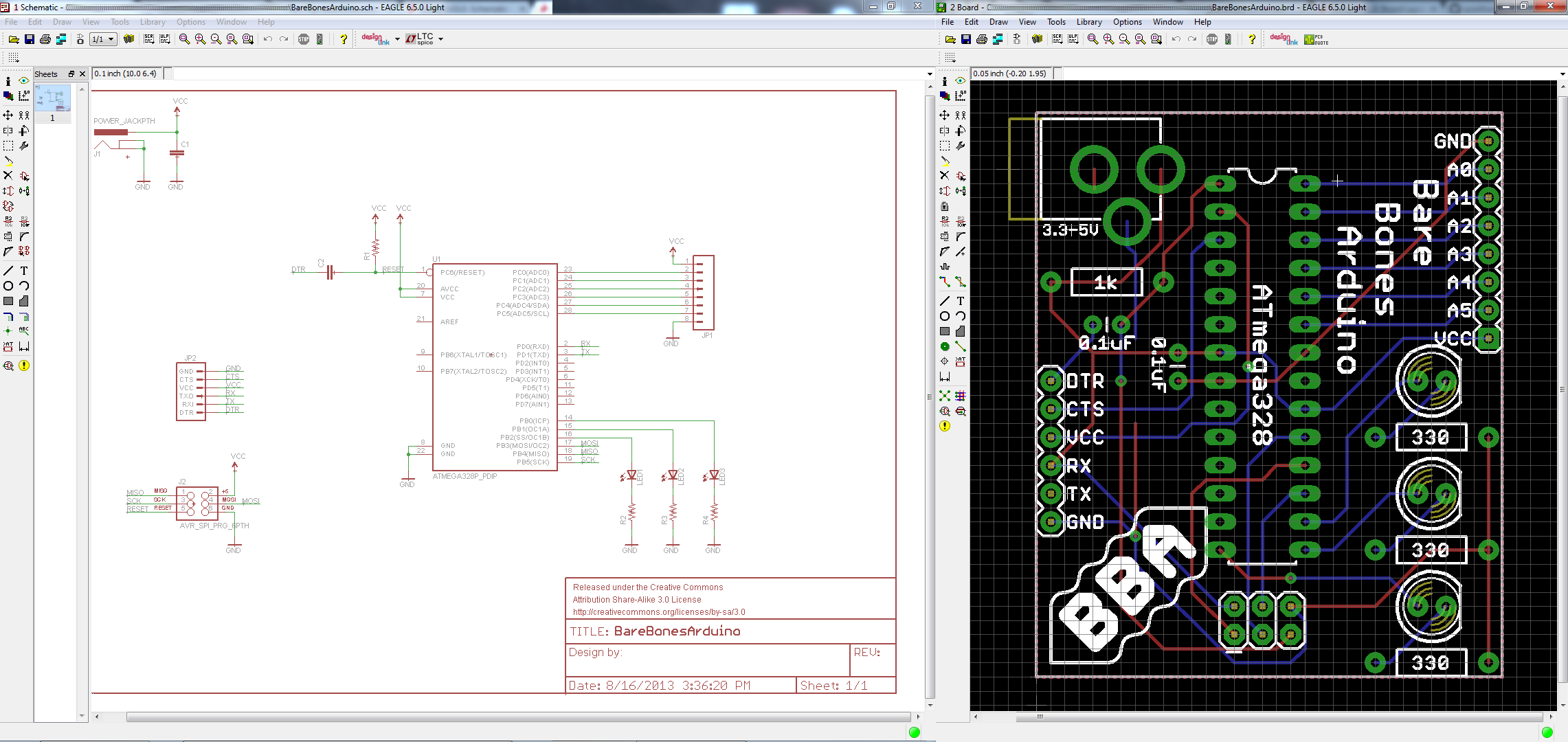
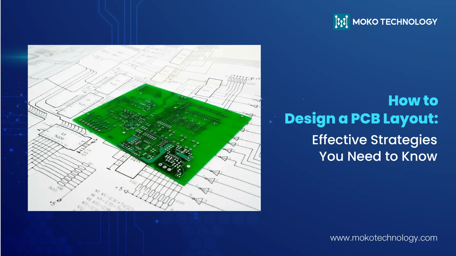
Schematic Diagram To PCB Layout: The Design Transition Guide - Convert schematic diagram to pcb layout
If you are searching about Pcb Board Design Guide at Santiago Vanmatre blog you've visit to the right web. We have 35 Pics about Pcb Board Design Guide at Santiago Vanmatre blog like Convert Schematic Diagram To Pcb Layout, From Schematic Diagram to PCB Layout: Simplifying the Design Process and also PCB Schematic vs PCB Layout Explained for Better PCB Design Process. Here it is:
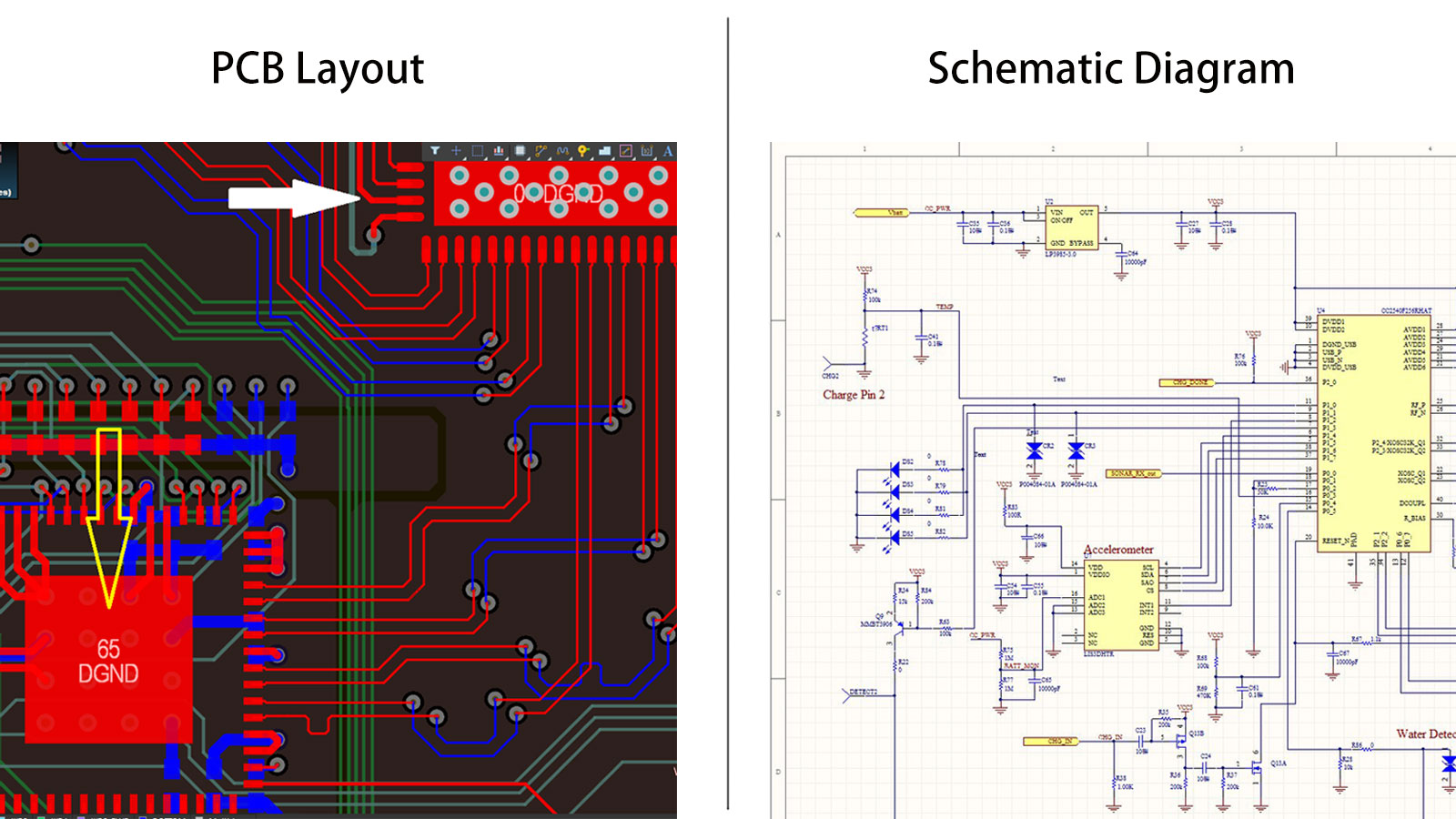
Pcb Board Design Guide At Santiago Vanmatre Blog
 storage.googleapis.com
Pcb Board Design Guide at Santiago Vanmatre blog
PCB Schematic Vs. PCB Layout: What's The Difference? - GlobalWellPCBA
 www.globalwellpcba.com
PCB Schematic vs. PCB Layout: What's the Difference? - GlobalWellPCBA
Characteristics Of Schematic To PCB And Complete Guideline To Draw It.
 swimbi.com
Characteristics of Schematic to PCB and Complete Guideline to Draw it.
RF PCB Design: A Practical Guide For Engineers | Viasion
 www.viasion.com
RF PCB Design: A Practical Guide for Engineers | Viasion
How To Design A PCB Schematic: A Step-by-Step Guide
 www.mokotechnology.com
How to Design a PCB Schematic: A Step-by-Step Guide
From Schematic Diagram To PCB Layout: Simplifying The Design Process
 elecschem.com
From Schematic Diagram to PCB Layout: Simplifying the Design Process
How To Design A Schematic - Circuit Diagram
 www.circuitdiagram.co
How To Design A Schematic - Circuit Diagram
A Detailed Guide To PCB Layout Design – PCB HERO
 www.pcb-hero.com
A detailed guide to PCB layout design – PCB HERO
Convert Schematic Diagram To Pcb Layout
 www.circuitdiagram.co
Convert Schematic Diagram To Pcb Layout
How To Design A PCB Schematic: A Step-by-Step Guide
 www.mokotechnology.com
How to Design a PCB Schematic: A Step-by-Step Guide
How To Convert Schematic Diagram Into PCB Layout? - Artist 3D
 artist-3d.com
How to Convert Schematic Diagram into PCB layout? - Artist 3D
What Is Circuit Board Schematic Diagram ? - RayPCB
 www.raypcb.com
What is circuit board schematic diagram ? - RayPCB
Pcb Schematic Design
 wiringdiagramexamples.blogspot.com
Pcb Schematic Design
Circuit Diagram To Pcb Layout Converter Online
 warholgoddessjx7guidefix.z13.web.core.windows.net
Circuit Diagram To Pcb Layout Converter Online
How To Design A PCB Layout
 hilelectronic.com
How to Design a PCB Layout
Pcb Board Design Guide At Santiago Vanmatre Blog
 storage.googleapis.com
Pcb Board Design Guide at Santiago Vanmatre blog
PCB Stackup Design Guidelines - MOKO Technology
 www.mokotechnology.com
PCB Stackup Design Guidelines - MOKO Technology
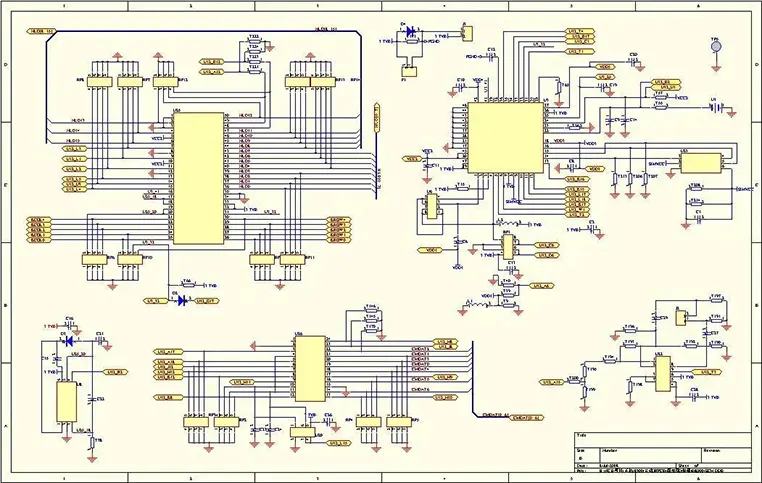
Schematic Diagram And PCB Design - General Guidance - Arduino Forum
 forum.arduino.cc
Schematic diagram and PCB design - General Guidance - Arduino Forum
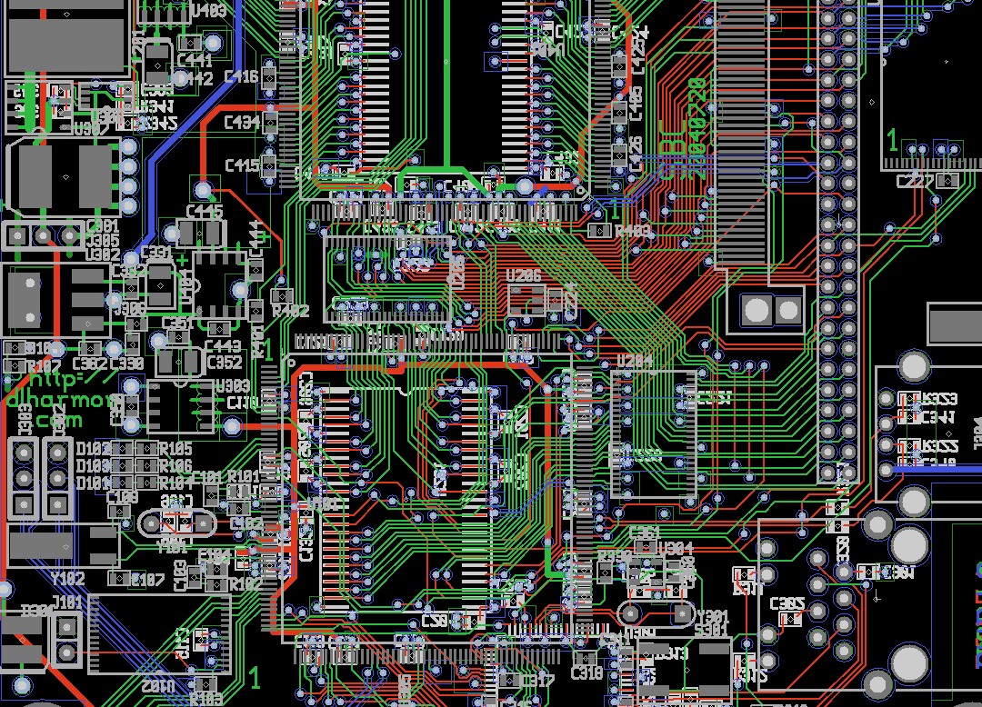
High Speed Pcb Layout Guidelines - Design Talk
 design.udlvirtual.edu.pe
High Speed Pcb Layout Guidelines - Design Talk
Guidelines For A Good Schematic Diagram Pcb Assemblypcb Printed Circuit
 fity.club
Guidelines For A Good Schematic Diagram Pcb Assemblypcb Printed Circuit ...
A Detailed Guide To PCB Layout Design - IBE Electronics
 www.pcbaaa.com
A detailed guide to PCB layout design - IBE Electronics
PCB Schematic Diagram Design And Manufacturing Best Practices- Jarnistech
 www.jarnistech.com
PCB Schematic Diagram Design and Manufacturing Best Practices- Jarnistech
A Detailed Guide To PCB Layout Design |Qtech Technology Co. Ltd
 qtech-us.com
A detailed guide to PCB layout design |Qtech Technology Co. Ltd
Guidelines For A Good Schematic Diagram Pcb Assemblypcb Low Volume PCB
 fity.club
Guidelines For A Good Schematic Diagram Pcb Assemblypcb Low Volume PCB
PCB Layout Design Guide: Tools, Steps, Rules & Best Practices
 www.ersaelectronics.com
PCB Layout Design Guide: Tools, Steps, Rules & Best Practices
PCB Schematic Vs. PCB Layout: What's The Difference? - GlobalWellPCBA
 www.globalwellpcba.com
PCB Schematic vs. PCB Layout: What's the Difference? - GlobalWellPCBA
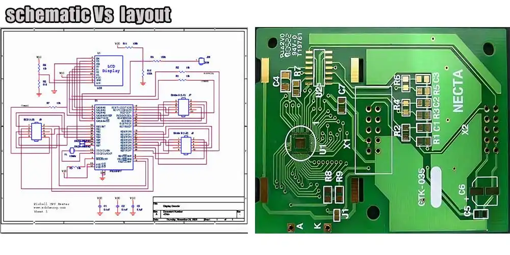
Pcb Layout Vs Schematic Diagrams » Wiring Diagram
 www.organised-sound.com
Pcb Layout Vs Schematic Diagrams » Wiring Diagram
Guidelines For A Good Schematic Diagram Pcb Assemblypcb Printed Circuit
 fity.club
Guidelines For A Good Schematic Diagram Pcb Assemblypcb Printed Circuit ...
PCB Schematic Vs PCB Layout Explained For Better PCB Design Process
 www.pcbmay.com
PCB Schematic vs PCB Layout Explained for Better PCB Design Process
Convert PCB Schematic Diagram Service-one-stop Solution
 hilelectronic.com
Convert PCB Schematic Diagram Service-one-stop solution
How To Read PCB Layout Design: Beginner’s Guide
 www.viasion.com
How to Read PCB Layout Design: Beginner’s Guide
What Is The Difference Between Schematic And Layout? – PCB HERO
 www.pcb-hero.com
What is the difference between schematic and layout? – PCB HERO
Your Guide To Perfecting The PCB Schematic Design – Hillman Curtis
 hillmancurtis.com
Your Guide to Perfecting the PCB Schematic Design – Hillman Curtis ...
PCB Schematic Vs PCB Layout
 www.nextpcb.com
PCB Schematic vs PCB Layout
PCB Schematic – A Professional Guide To Design And Layout - PCBA
 www.pcba-manufacturers.com
PCB schematic – a professional guide to design and layout - PCBA ...
pcb board design guide at santiago vanmatre blog. A detailed guide to pcb layout design |qtech technology co. ltd. How to read pcb layout design: beginner’s guide